Xiaomi Shows AI Cube Prototype: Three Chips, 1.22TB/s


Xiaomi unveiled the AI Cube Prototype at its Xuanjie chip technical briefing on August 24, 2026 — an engineering-sample mini PC built around three of the company’s own chips at once, aimed squarely at running large language models locally. The headline number is the 1.22 TB/s bandwidth of the new Xuanjie O100 accelerator, but the more interesting detail is how Xiaomi splits bandwidth and capacity across three separate dies instead of one unified memory pool.
Intermediate


Three Chips, Three Jobs
The Cube combines the Xuanjie O3, O100 and D100 — announced the same afternoon as a set that Xiaomi describes as the compute foundation for its “human–car–home” ecosystem. Each chip does something different:
- Xuanjie O3 — the flagship SoC, built on a 3nm process with 24 billion transistors. It uses a ten-core all-big-core CPU (six ultra-large plus four large cores) at up to 4.35 GHz, a 16-core G2-Ultra NX GPU, and 16 MB of SLC cache. Xiaomi says it is the first mobile processor to support LPDDR6, reaching 113.8 GB/s — a 48% bandwidth gain over the O1. Its rebuilt NPU delivers 200 TOPS of tensor compute and 3.13 TFLOPS of vector compute, and Xiaomi states it was designed specifically for its own MiMo on-device models.
- Xuanjie O100 — a dedicated high-bandwidth AI accelerator, and the source of the 1.22 TB/s figure. Xiaomi calls it the industry’s first 6nm AI accelerator using wafer-on-wafer 3D stacking, joined by hybrid bonding at a 1.4 µm pitch, yielding 28,672 effective data lines and a 14-core high-bandwidth NPU. Xiaomi quotes on-device inference of up to 330 tokens per second.
- Xuanjie D100 — a 3nm automotive-grade AI chip with a 20-core CPU and 16-core NPU. This is the capacity chip: it supports up to 160 GB of unified memory and, per Xiaomi, local deployment of models up to 200B parameters.
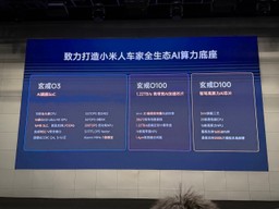
Where the 1.22 TB/s Actually Lives
Read quickly, the specification sheet looks contradictory: 1.22 TB/s of bandwidth next to 160 GB of memory would be an extraordinary combination. Those numbers belong to different chips.
Xiaomi’s own wording is precise — the O100 figure is near-memory compute bandwidth (超高近存计算带宽), the throughput available to memory stacked directly onto the accelerator die. That kind of bonded, wafer-stacked memory buys enormous bandwidth at limited capacity. The 160 GB of unified memory sits on the D100 instead, where capacity is the point and bandwidth is not quoted. The O3 handles general-purpose work at 113.8 GB/s.
The comparison Xiaomi draws is worth reading carefully too: the O100 is said to have 16 times the bandwidth of a “traditional flagship phone.” That implies a baseline near 76 GB/s — a conventional LPDDR5X flagship, not Xiaomi’s own new O3. Measured against the O3’s LPDDR6 figure, the multiple is closer to 10.7×.
This is a different design from the single large unified-memory pool used by Apple’s M-series or AMD’s Ryzen AI Max parts. It also explains the Cube’s stated software model: 120B and 3B models deployed together, with what Xiaomi calls fast–slow system switching — a small model on the low-latency path and a large one for harder queries.
What This Means
For anyone tracking local inference hardware, the O100 is the part to watch. Memory bandwidth, not compute, is the binding constraint on single-user token generation, and wafer-level stacking is a credible way to attack it — the same reasoning behind high-bandwidth memory in data-centre accelerators, applied at edge power budgets. A 150W sustained power envelope in an aluminium chassis is a very different thermal class from a rack GPU.
Several things remain unstated. Xiaomi has not disclosed how memory is partitioned across the three chips, what quantization the 120B model runs at, or how the 330 TPS figure was measured. There is also a timing constraint: Xiaomi says the O3 has entered mass production and debuts in the Xiaomi 18 Fold in September, but the O100 and D100 have only completed development and are slated for commercial use next year. A shipping Cube cannot precede them. No price or release date has been announced, and Xiaomi labels the unit a prototype.
Related Coverage
- Xiaomi Releases MiMo-V2.5-Pro: 1T-Parameter Open MoE Matches Frontier Coding Models — the model family the O3’s NPU is explicitly designed around
- Qwen3.8-27B: Frontier Agentic Scores on a Single Consumer GPU — the software side of the same trend toward capable local models
This post was drafted with AI assistance and reviewed by RITS staff.
Sources
- 小米 AI Cube 工程版迷你主机官宣:玄戒 O3+O100+D100 三芯阵容,150W 持续性能释放 — IT之家, August 24, 2026
- 行业首颗 6nm 3D 晶圆级堆叠的 AI 加速芯片:小米玄戒 O100 官宣 — IT之家, August 24, 2026
- 国内首款 3nm 智驾芯片,小米玄戒 D100 官宣明年商用 — IT之家, August 24, 2026
- 首个突破 500 万分的旗舰 SoC!小米玄戒 O3 正式发布,CPU 采用十核全大核设计 — IT之家, August 24, 2026
- 小米玄戒三芯集结:O3 开启规模量产、O100 和 D100 研发完成明年商用 — IT之家, August 24, 2026


 沪公网安备31011502017015号