IntermediateAI
The 8 GB Accelerator That Becomes 64 GB: cmpunlocker v0.5
- AI Chips
- local inference
- nvidia
- open source
On 5 October 2026, the open-source project cmpunlocker released version 0.5, adding error-correcting code (ECC) on both DRAM and SRAM, and four more streaming multiprocessors (SMs), to a card it has spent more than a year re-enabling: the NVIDIA CMP 170HX. The board is a GA100 accelerator — the same Ampere die that sits in an A100 — sold in 2021 in a deliberately restricted configuration and since retired. Stock, it reports 8 GB of memory and a fraction of its compute throughput. Unlocked, it reports 64 GB of HBM2e and runs 27-billion-parameter models locally at rates that put it in the same conversation as hardware costing several times as much.

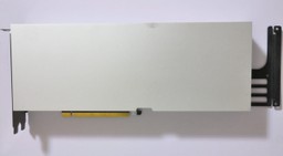
A complete die, deliberately clamped
Physically the CMP 170HX is a full GA100: 54.2 billion transistors on an 826 mm² TSMC 7nm die, 70 SMs, 4,480 CUDA cores, 32 MB of L2 cache, and a 4,096-bit HBM2e memory bus rated for 1,493 GB/s. Almost none of that is visible through the driver. Firmware and one-time-programmable (OTP) fuses clamp the memory controller to 8 GB — or 40 GB on the 10 GB variant — disable whole clusters of SMs, throttle FP32 arithmetic to roughly 0.4 TFLOPS, and hold the PCIe link at Gen1 ×4, about 1 GB/s. The restrictions are re-imposed on every boot, enforced during the power-on sequence run by the GPU’s own system processor.
How the unlock works
cmpunlocker does not flash or modify the card. It patches NVIDIA’s open-source Linux kernel modules — nvidia.ko and nvidia-drm.ko — so that the driver reconfigures the GPU during GSP (GPU System Processor) boot, before the fuses take hold. The patched modules open the Booter’s program-logic-module permissions, then write the registers that define memory geometry (CFG1 and LMR) and SM suspension state (SS0 and SS1). Because the change lives in the driver rather than in the hardware, it re-applies on every module load and survives reboots; nothing is written to the card’s VBIOS.
The cost is operational rather than financial. It is Linux-only and requires root, kernel headers matching the running kernel, NVIDIA’s open driver, and Secure Boot disabled — the patched modules are unsigned. A routine driver upgrade silently undoes the unlock, so the community documentation recommends pinning the driver tree and warns that stock DKMS modules can shadow the patched ones on Ubuntu-class hosts. PCIe Gen2 is itself a software unlock, added in v0.2; reaching more than four lanes requires soldering 24 AC coupling capacitors to the board. An 80 GB profile for the 10 GB cards was built, tested, and rejected as unstable.
What it runs
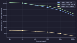
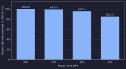
The community’s CMP 170HX documentation project publishes a sweep of 1,603 decode points from a single unlocked card at 300 W. Coding-style prompts at 16k context decode at 227.7 tokens/s with a 30B mixture-of-experts model at W4A16 in vLLM, at 1.7 s time-to-first-token; at 64k context the same model holds 217.9 tokens/s. Sixteen concurrent streams at 32k prompts aggregate 1,306 tokens/s. Median decode retains 96.2% of its 1k-context rate at 16k and 79.4% at 128k, and dropping the power limit to 200 W costs only 4.3%.

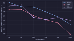
Compute is what the unlock transforms. FP32 climbs from 0.41 to 12.99 TFLOPS, FP64 from 0.19 to 6.44 TFLOPS, and INT8 from 1.64 to 48.03 TFLOPS, while FP16 is untouched at 49.05 TFLOPS. But capacity, not throughput, is the reason to buy: 64 GB of HBM2e holds a 70B-class model at 4-bit with room to spare, and even gpt-oss-120B at 4-bit just fits. For comparison, listings put an 80 GB A100 at $18,999 and a 64 GB AMD MI210 at $5,042.

Where it falls short
The host link is the weak point. Even at Gen2 ×4, a single card moves roughly 2 GB/s, so loading 64 GB of weights takes tens of seconds and tensor-parallel scaling across cards is bottlenecked by the interconnect. A four-card configuration has been measured at about 98 tokens/s on a 284B-parameter mixture-of-experts model, using pipeline parallelism, where only hidden states cross the link. There is no NVLink — the connectors are present but fuse-disabled — no display output, and no Windows support, because the unlock path is Linux-specific. The boards are passively cooled and need forced chassis airflow, and NVIDIA supports none of it.

What This Means
An unlock like this one matters less as a buying recommendation than as a signal about where capable silicon ends up. A retired accelerator with datacenter-class memory bandwidth is being returned to service by a small open-source project and a community documentation effort — at a moment when demand for local inference capacity runs well ahead of what many research groups can afford to buy new. The release history also shows the work is cumulative: memory geometry first, then PCIe, then BAR1 and profiling in v0.4, and now ECC in v0.5, closing one of the gaps that made the unlocked card awkward for long-running use.
What has not changed is equally worth stating. The unlock restores capacity and bandwidth the silicon always had; it does not make the card fast, and even unlocked its throughput sits below an A100’s. It is a systems project, not a product — best read as evidence of how much usable accelerator capacity now circulates outside the official market, and how thin the support is for anyone who wants to use it.
This post was drafted with AI assistance and reviewed by RITS staff.
Sources
- cmpunlocker v0.5 release notes
- cmpunlocker repository
- CMP 170HX Documentation — Unlock Overview
- CMP 170HX Documentation — Performance Overview
- NVIDIA CMP 170HX full specifications (170th Street)
- CMP 170HX 64 GB price and local LLM reference
- Community measurements on multi-card CMP 170HX configurations — NVIDIA Developer Forums
- Academic study of CMP 170HX compute reuse and energy efficiency (arXiv:2505.03782)



 沪公网安备31011502017015号